Project Detail
Thermal Redesign Journey
A deployed product was generating field returns at a rate that threatened its commercial viability. I led a structured two-phase thermal redesign. I fixed the airflow path first, then the internal thermal stack, rather than reaching for a workaround.
Both phases shipped to production. Chip operating temperature dropped by 16°C and field returns came down to under 3%. The new thermal headroom also unlocked a 50% increase in operating power and a 33% reduction in treatment time, making the redesigned product both more reliable and more effective than its predecessor.
At a glance
Skills & tools
Outcome
Both phases shipped to production. −16°C chip temp, field returns under 3%, +50% operating power vs previous generation.

Original model
Chip temperature across four grill geometry iterations. Each curve benchmarked against the original design. Concept 3 delivered the largest reduction and was selected for physical validation.
Key outcomes
-16°C
Chip temperature reduction
<3%
Final field return rate
+50%
Operating power vs previous gen
-33%
Treatment time for the user
Skills applied
Disclosure: Specific baseline metrics, proprietary simulation outputs, and product identifiers have been withheld or generalised in line with confidentiality obligations. The temperature comparison chart, airflow simulation images, and heatsink images are non-proprietary. All outcomes stated are directionally accurate.
The problem
A deployed product was overheating in the field
Field returns had climbed past a commercially viable threshold. Root cause analysis pointed to a single structural issue: the enclosure grill geometry was restricting airflow, causing heat to accumulate at the chip faster than the thermal path could dissipate it.
The temptation was to adjust thermal limits in firmware. Instead, I used 5 Whys and 8D to scope the real problem, and committed to fixing the physical thermal path across two design phases.
Root cause chain
Restrictive grill geometry
Original enclosure design
Reduced airflow
Through the enclosure
Heat accumulation
Chip exceeds design limits
Thermal failure
Component shutdown
Field return
Customer-reported
Phase 1
Airflow path redesign
The grill geometry was the primary restriction. I ran a SolidWorks Flow Simulation baseline on the existing design, then developed three alternative grill geometries, varying slot dimensions, pattern density, and effective open area. All four options were evaluated on thermal performance, velocity contours, and manufacturability before selecting one for physical validation.
Baseline
ReferenceOriginal circular grill pattern. Sets the reference for airflow velocity and chip temperature. All concepts benchmarked against this.
Concept 1
IterationIncreased slot density. Moderate thermal improvement over baseline. Some DFM constraints flagged during review.
Concept 2
IterationWider slot geometry with higher open area. Better airflow, but introduced structural trade-offs in the housing wall thickness.
Concept 3
Selected ✓Optimised slot width, pitch, and orientation. Best thermal result across all iterations. Manufacturable. Selected for physical validation.
SolidWorks Flow Simulation: velocity contours
Baseline
Reference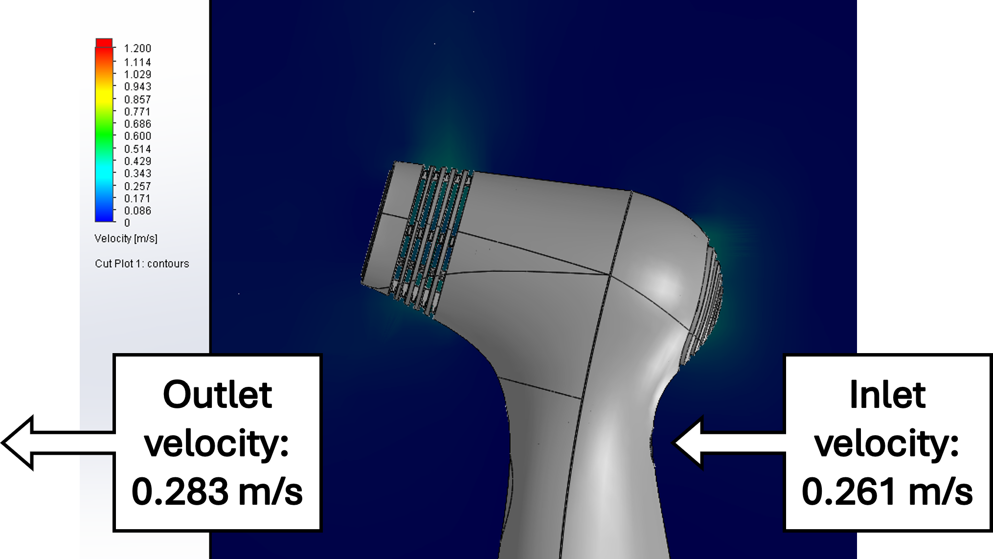
Concept 1
Iteration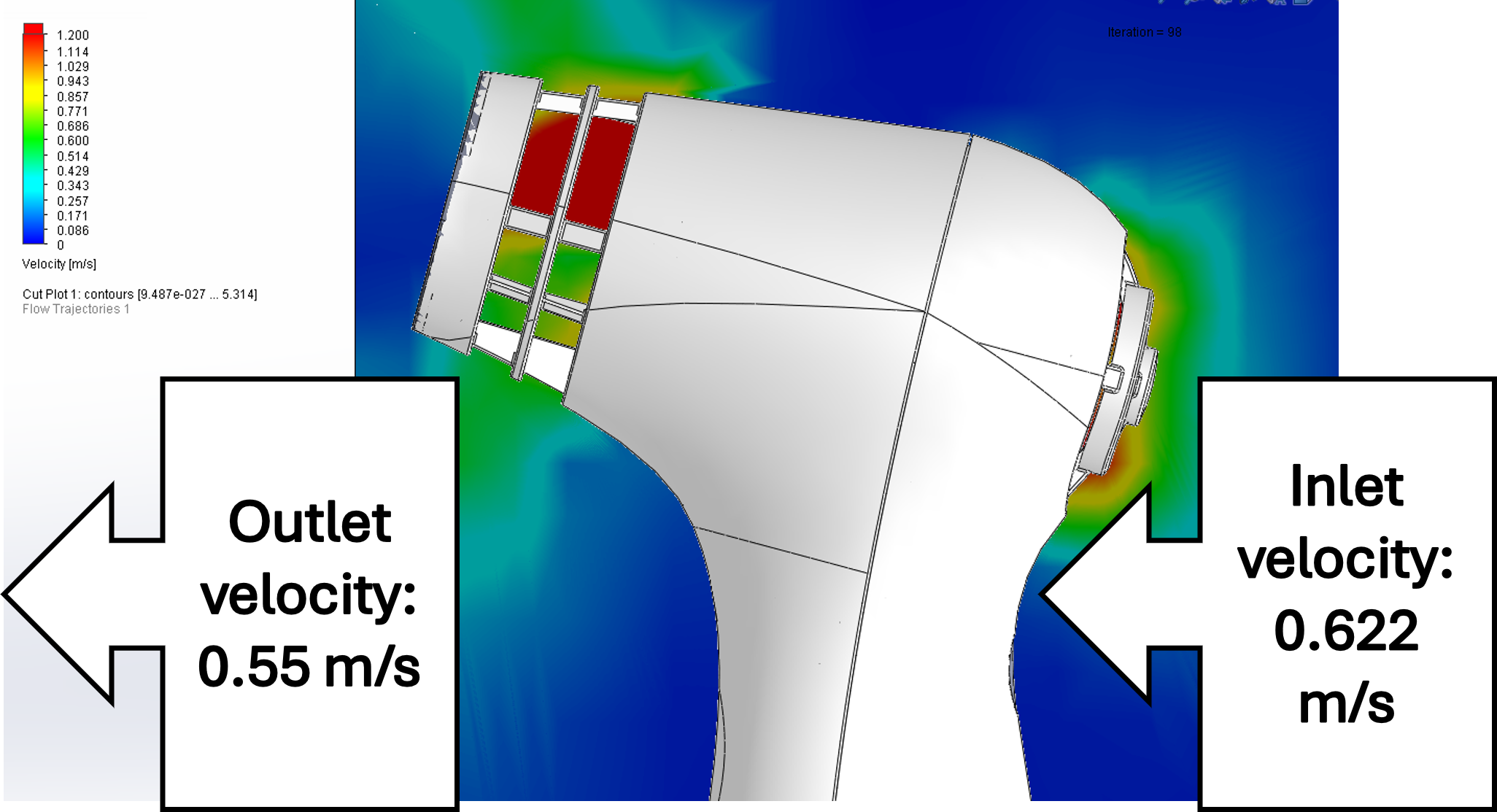
Concept 2
Iteration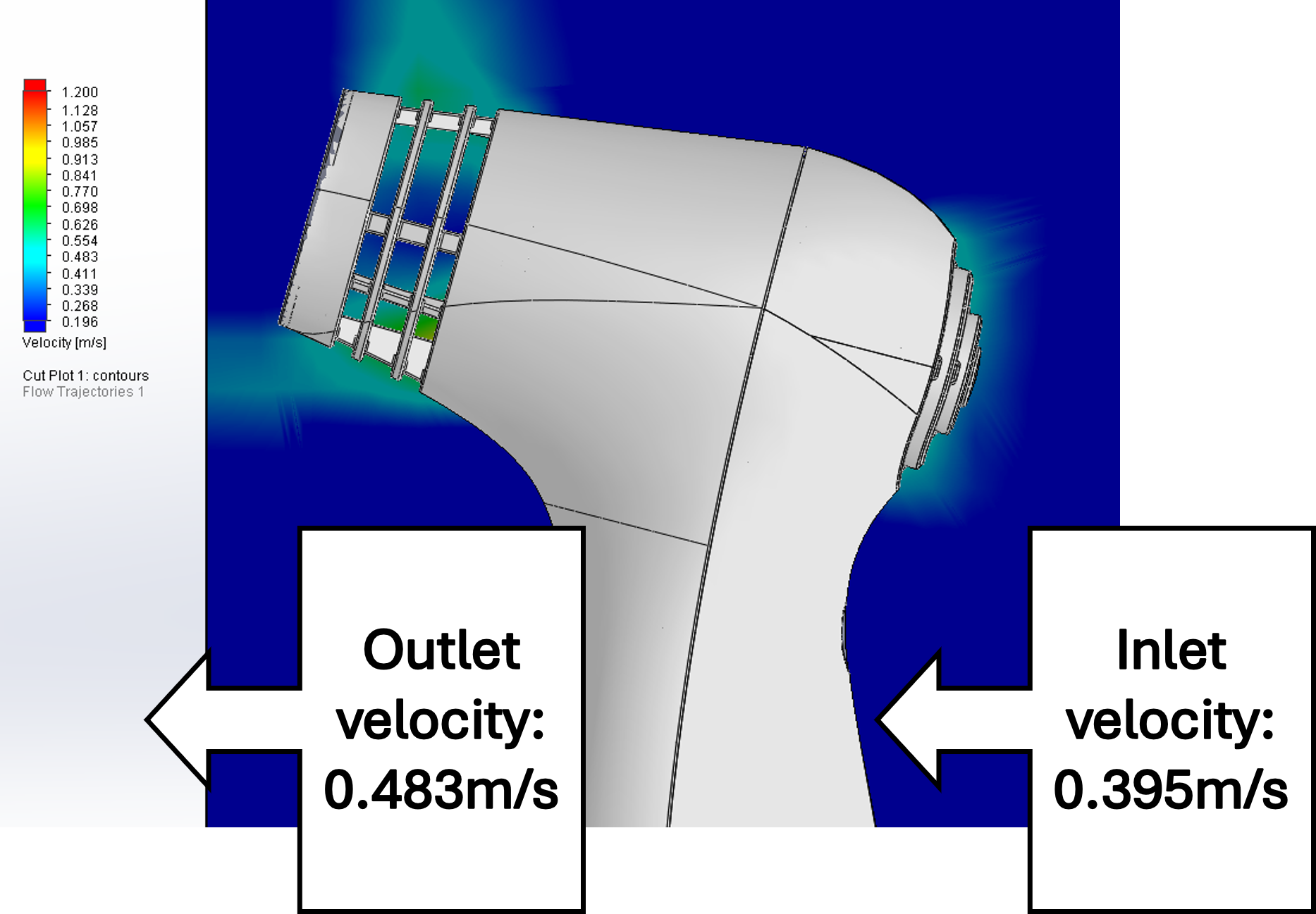
Concept 3
Selected ✓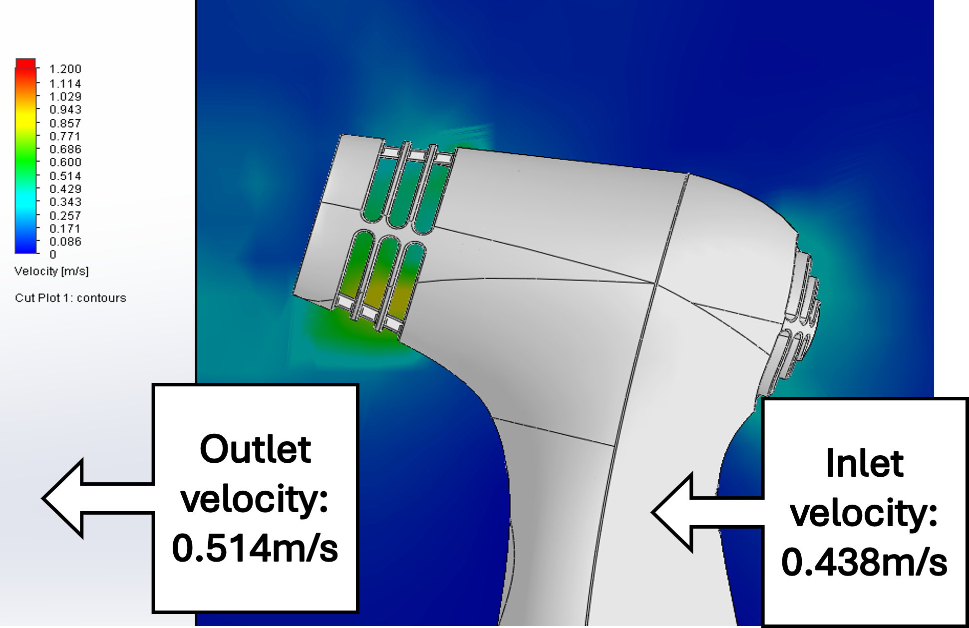
Velocity contour comparison across all four grill geometries. Higher outlet velocity = better airflow through the enclosure.
Phase 1 result
Concept 3 was physically validated. Chip temperature dropped by 10°C and field returns fell by more than half. That was a meaningful result, but not enough. Simulation and physical data both pointed to a remaining bottleneck in the internal thermal stack. Phase 2 was scoped.
Field return rate
>50%
reduction vs pre-redesign baseline
Chip temperature
−10°C
Physical testing confirmed
Status
Shipped
Validated & in production
Phase 2
Internal thermal stack upgrade
Improved airflow reduced the thermal load, but the junction-to-case path itself was still the limiting factor. Phase 2 applied two targeted design changes: a more efficient semiconductor source and a fully redesigned conduction path to the enclosure. Together, they didn’t just stabilise the existing product. They created enough thermal headroom to run at significantly higher operating power, unlocking a step-change in product performance.
Design Change 1
Semiconductor package swap
Through structured supplier evaluation I identified a thermally efficient chip that ran cooler under the same operating conditions, addressing the bottleneck that improved airflow alone couldn’t fix. The new component dissipated heat more effectively at source, and critically, its thermal stability also meant it could sustain 50% higher output power while staying within its thermal envelope, something the previous chip could not support.
Method
Supplier evaluation + datasheet analysis
Key parameter
Junction-to-case thermal resistance (Rθjc)
Risk managed via
FMEA + physical validation
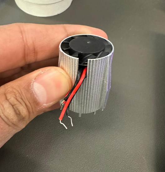
Design Change 2
All-metal heatsink path
Replaced a hybrid plastic-metal thermal interface with a fully metallic conduction path from chip to enclosure. Eliminating the non-conductive material in the stack removed the thermal resistance that was preventing the chip from shedding heat effectively, regardless of airflow improvement.
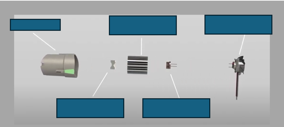
Left: engine with plastic plenum. Right: all-metal plenum engine.
Phase 2 result
Both design changes were physically validated. The updated stack brought field returns to under 3%, a commercially sustainable threshold, and held up under extended test conditions.
Field return rate
<3%
Final production state
Additional chip ΔT
−6°C
On top of Phase 1 reduction
Status
Shipped
Validated & in production
What the redesign unlocked
From fixing a failure to enabling a better product
The thermal fix wasn’t the end of the story. With a lower-resistance semiconductor and a fully metallic conduction path, the product could sustain substantially higher operating power without approaching thermal limits. That headroom was used to upgrade the product’s output, delivering a more effective treatment in less time, while remaining thermally stable at load levels the previous generation could not reach.
Operating power
+50%
Sustained at thermal stability vs previous generation
Treatment time
−33%
Faster session for the user, same or better efficacy
Product outcome
More effective. More reliable.
Thermally stable at elevated power across both phases